
Photolithographic procedures are used to fabricate a variety of microstructures such as microfluidic channels, micromoulds and microelectrodes. Two types of photoresist are used:Microfabrication Techniques
We have an in-house facility for standard microfabrication procedures such as photolithography and soft lithography. Using these facilities it is possible to fabricate features with characteristic dimensions in the order of 1 μm.
Photolithography
Photolithographic procedures are used to fabricate a variety of microstructures such as microfluidic channels, micromoulds and microelectrodes. Two types of photoresist are used:
Negative resist
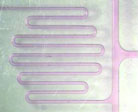
Typically used to create microchannels and micromoulds using the process shown below.

A thin film of negative resist (usually SU-8) is exposed to UV light through a computer generated mask. This causes the exposed areas to cross-link; any areas which are not exposed are removed by immersion in developer solution.
Positive resist
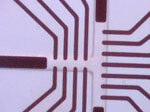
Typically used to create microelectrodes using the process shown below.

A thin film of positive resist is exposed to UV light through a computer generated mask. The areas that are exposed become more susceptible to the developer solution. The wafer can then be coated with metals such as gold, silver and platinum using an evaporator. The wafer is then immersed in acetone to remove any positive resist and reveal the microelectrode pattern. One of the main benefits of this approach is the ability to accurately align microfeatures such as electrodes and channels, as shown in the figures below.
 |
 |
|---|---|
| Image of a microfluidic device | Image of a microfluidic device containing electrodes |
Soft Lithography
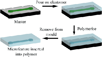 A schematic illustration of replica moulding soft lithography is shown left. A micromould (typically produced by photolithography) is covered in a liquid polymer (such as poly(dimethylsiloxane) PDMS) and the polymer allowed to cure, the polymer is then peeled off the micromould to reveal the microstructure. This enables the accurate reproduction of a microfeature and reduces the cost of the fabrication procedure. Additionally, the polymer used can be tailored to the final application; i.e. solvent resistant, non-fluorescent, hydrophilic/hydrophobic etc.
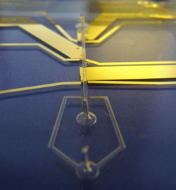 The microchannels produced by the soft lithographic process can also be aligned with microelectrode features on another wafer and sealed using a plasma bonding process. An example of such a device is shown right.