The advantages of using small scale electrodes for voltammetric applications has been well-established and we have been involved in projects seeking to exploit the improvements in nanofabrication and numerical simulation techniques in order to provide a quantitative insight into the processes occurring at the electrodes.
Motivation
One of the key motivations to developing a nanoeletrode voltammetric technique is the ability to apply this methodology to systems which can no longer be studied by conventional measurement techniques. For example the imaging of nanostructured materials becomes more difficult when the feature size is less than the wavelength of light. By using a voltammetric approach, the size and position of an object can be determined. This technique is contingent on the development of both experimental techniques and numerical models appropriate on the nanoscale.
Nanofabrication
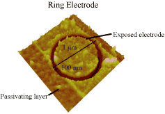
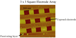
Fabrication of the nanoelectrodes is performed using some standard photolithographic techniques to produce a microelectrode with a passivating layer and then using focused ion beam (FIB) etching to remove some of this passivating layer. FIB etching works by directing a focused beam of gallium ions onto a substrate, this can then be used to remove surface material; the depth of the feature produced is dependent on the duration of the etch and the size of the feature to be formed. The images below show some AFM images of nanoelectrodes fabricated using FIB etching.


Numerical Simulation Techniques
The AFM images above clearly show that at this scale the increased significance of surface roughness relative to the feature size; as a result an alternative numerical modeling technique, which can more easily incorporate such features, was sought. The lattice Boltzmann technique has been developed for electrochemical applications to aid the design and quantification of these nanofabricated devices.
Voltammetric Detection
Due to the low current response observed with single nanoelectrodes with standard voltammetric techniques, arrays of nanoelectrodes were initially tested. Using these arrays in addition to lattice Boltzmann simulations the affect of a number of parameters such as interelectrode separation and passivation layer height could be studied. In order to further interogate these nanoelectrodes, more sensitive voltammetric approaches are required. One such method is AC voltammetry which is the subject of an on-going collaboration with Prof. Alan Bond.

